There are several basic methods for interfacing Keypads to microcontrollers
or computers:
(Thanks to Stef Mientki for these nice pictures)
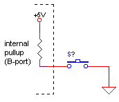 One pin
per switch.
One pin
per switch.
Multiple keys can be decoded.
If no internal pull-up resistor present, connect an external pull-up resistor (10 kOhm ... 100 kOhm).
Debouncing should be done in software and or using a smitt-trigger input. In some documents it's suggested to use a capacitor across the switch to reduce debouncing, this will do only harm because the edges of the signals are made slower, which is bad for digital circuits.
Example:
Switches can be shared with the data lines on standard 44780 LCD Panels as long as they are connected via a large resistor to the data line pin and then on to the controller so that if they are pressed while writing data to the LCD, the signal from the controller can "override" the effect of the switch.
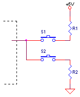
One pin for every two switches.
Only one switch at a time can be decoded.
External resistors are required. The circuit may be sensitivity to external electric noise. The port used must be able to act both as an input and output. The working is based on the parasitic capacitance of the port.
Decoding is done as follows:
If both readings were low, S2 is pressed If both readings were high, S1 is pressed If both readings were different nothing was pressed. By choosing one of the resistors much larger than the other, you can determine which key has precendence if both keys are pressed. The resistor values must be high so that excessive power draw is not caused when both switches are pressed.
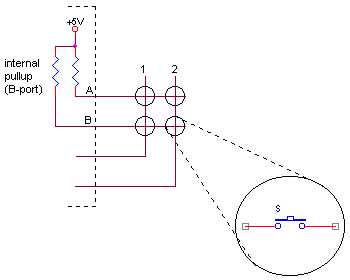
One pin plus a pin per switch pair (LCD panel compatible). Dwayne Reid contributes this great trick for reading sets of mutually exclusive switch pairs (up/down, left/right, etc...) which can also nicely co-exist with the standard 44780 LCD panels:
If you need more switch inputs, you can use a little trick I use. The pull-up resistors are a SIP bussed resistor network - I usually use 4k7. The common pin on the SIP goes to the PIC pin driving the R/S line on the LCD. The rest of the pins on the SIP connect to the switches. As usual, series resistors from the switches to the LCD data lines and thus to the PIC.Here's the trick: the switches are momentary, center-OFF switches: either toggle or rocker. The top row of switch contacts all connect to Vdd, the bottom row of contacts all connect to ground. The center contact of each switch goes to the SIP and the LCD data lines.
Set the RS line HI, read the switch inputs, save. Now set the RS line LO, read the switch inputs, save in another register.
Compare the registers. If a bit is LO in both registers, that switch is in the GND position. If a bit is HI in both registers, that switch is in the VDD position. If that bit is different in both registers, the switch is in the middle position.
I use three of those switches for up/down, left/right, escape/enter adjustments in my menu structure. The other switch is used for whatever else I might need. Notice that both functions on each switch are mutually exclusive - you have no need for the UP button if you are pressing the DOWN button. Same for left/right and enter/escape.
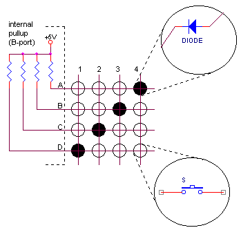
Most keypads are decoded via a matrix of rows and columns where each row or column is connected to a seperate IO pin on the processor and a switch or switch and diode is placed at all or most intersections between rows and columns.
 A matrix
of N columns by N rows supports N*N switches and requires 2*N IO pins
A matrix
of N columns by N rows supports N*N switches and requires 2*N IO pins
N = 1 / 2 / 3 / 4 ==> 1 / 4 / 9 / 16 switches
Multiple keys can be decoded.
Pull-up or pull-down resistors are necessary, if not provided internally by the processor
Each column is energized in turn and the rows are read to sense the closed key switches.
Example:
A matrix of N columns by N rows supports 2N * 2N - 2N switches
N = 1 / 2 / 3 / 4 ==> 2 / 12 / 30 / 56 switches
Multiple keys can not be decoded (just detected)
Pull-up or pull-down resistors are necessary, which are available on the B-port of most PIC-devices.
For values of N > 1, some multiple switch combinations can be resolved unambigious, others not.
In general use this design only when there's only 1 keypress at a time. The software should then check if just one key is pressed, otherwise wait till only 1 key pressed.
Example:
In the design shown here, each IO pin is typically left as an input with the pull up resistor enabled. Each IO pin is then set as an output, and pulled low and the other pins are read to detect that low signal being transfered via a closed keyswitch.
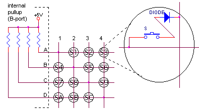
Another method requires additional diodes (one for each switch) but allows multiple keys to be unambigious decoded.
Pull-up or pull-down resistors are necessary, which are available on the B-port of most PIC-devices.
We can see how this design is decoded in the following table:
| When: | If Ain | If Bin | If Cin | If Din |
| Aout = 0 | X | =0? S4 | =0? S7 | =0 ?SA |
| Bout = 0 | =0? S1 | X | =0? S8 | =0? SB |
| Cout = 0 | =0? S2 | =0? S5 | X | =0? SC |
| Dout = 0 | =0? S3 | =0? S6 | =0? S9 | X |
Analog
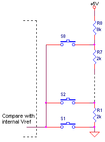
When it is very important to save IO pins, and the processor has an analog to digital converter built in, many keys can be detected by connecting them to the different points in a voltage divider.
Multiple keys can not be detected and will give a strange result.
The resistors under the top one can be replaced with forward biased diodes (since each will drop a small amount of voltage, acting as low value resistors) so that when multiple keys are pressed, only the lowest one will be detected.
Example:
Samuel Kerem [samuelkerem at juno.com] of Patton Electronics Co., 7622 Rickenbacker Dr., Gaithersburg, MD 20879 says:
...Looking at the figure, you'll notice a familiar 4x4 keypad with a single difference--each row and column are separated by a resistor. If key #1 is pressed, the resistance between nodes A and B (R1AB) is equal to 1.5*R; for key #2--R2AB = 1.5*R+R = 2.5*R; and so on ... key #N--RNAB = N.5*R. This variable resistor network is connected to a 555 timer (CMOS version), configured as an oscillator with the period of oscillation equal to T = 1.4*RAB*C, directly proportional to RAB.
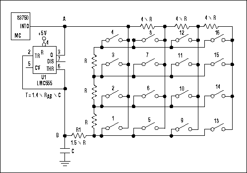
The oscillator runs only when a key is pressed, causing an interrupt request for the microcontroller. The INT0 pin is set up as edge-sensitive. The general algorithm can be described as: 1) after detecting the edge on the INT0 pin, wait 20 ms to eliminate ringing; 2) detect the next edge and start the internal timer; 3) the following edge stops the internal timer. The measured period (the time between two consecutive positive edges) will define the key number. Any microcontroller with a built-in timer (the vast majority of microcontrollers) can implement this idea.
Some possible sources of errors in this application are: 1) component tolerances; 2) 256.6 5s instead of 256 for 1% resistors; 3) the closest value to 4*R, if R = 3.9k, will be 15.4K or 15.8K instead of the calculated 15.6k., an additional 1% error for each following column; 4) the 555 oscillator inaccuracy--temperature drift of 75 ppm/C0 and variation 0.03% for a power- supply variation of 10.1 V The value for R1 =1.5*R is chosen to provide the highest error margin for the elements by moving the period value in the middle of two consecutive numbers.
Dedicated chip
Of course, there are keyboard decoder chips available.
Todd Peterson says
You might have a look at our EDE1144 4x4 matrix keypad encoder IC. It will allow you to read all sixteen keys using a single I/O pin, and adds features such as key debouncing, keybeep, and automatic repeat when a key is held. A datasheet is available at http://www.paladinsemi.com/keypad-interface.phpOne tremendous advantage to using the EDE1144 over other keypad IC's is that the keys are NOT continuously scanned (continuos scanning can cause unintended radiation from the wires leading to the keypad). Instead, stable voltages are held on the keys and a query cycle scans once per keypress.
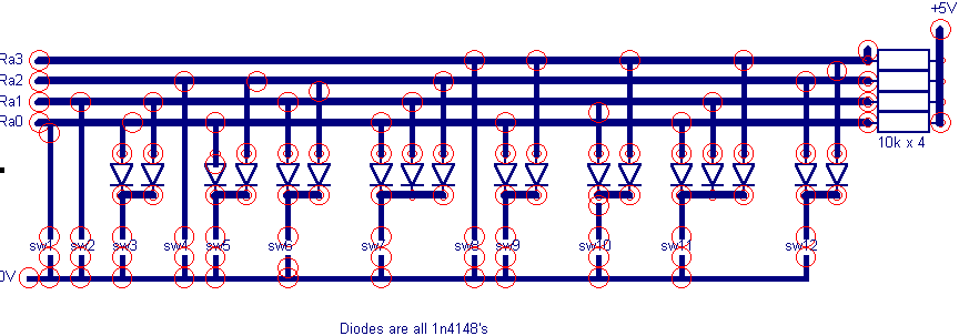
John Perkinton (jperk at TAYNET.CO.UK) drew up this schematic of his keyboard encoder.
Also:
See also:
| file: /Techref/io/keyswitch.htm, 12KB, , updated: 2023/9/13 13:59, local time: 2025/5/21 06:36,
3.149.27.125:LOG IN
|
| ©2025 These pages are served without commercial sponsorship. (No popup ads, etc...).Bandwidth abuse increases hosting cost forcing sponsorship or shutdown. This server aggressively defends against automated copying for any reason including offline viewing, duplication, etc... Please respect this requirement and DO NOT RIP THIS SITE. Questions? <A HREF="http://www.sxlist.com/techref/io/keyswitch.htm"> Key Switch Encoding / Decoding</A> |
| Did you find what you needed? |
Welcome to sxlist.com!sales, advertizing, & kind contributors just like you! Please don't rip/copy (here's why Copies of the site on CD are available at minimal cost. |
|
The Backwoods Guide to Computer Lingo |
.