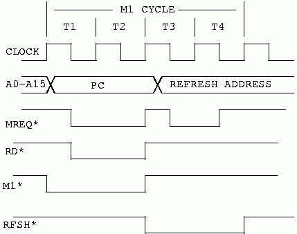
In an ideal world The Z80 would present us with only one set of timing for memory. Unfortunately, the world is not ideal. The Z80 CPU uses memory for two types of operations; instruction fetches, and data store/retreival. The timing for these operations is not the same. The following drawing shows an instruction fetch, or M1, cycle.
Figure 21 shows a Z80 instruction fetch. It lasts for four processor clock cycles. During the first two clocks, the actual instruction is fetched from memory. During the last two clock cycles, the Z80 decodes the instruction internally, while it refreshes DRAMs externally.
As we can see in figure 21, we actually have one and a half clocks for memory access during an instruction fetch. MREQ* goes low, active, with the first falling edge of the processor clock. This is called T1, or time 1. It goes back high at the end of T2, the second rising clock edge in the M1 cycle. This signals the end of the memory access for the instruction fetch. We actually have to get the data to the CPU chip sometime before the rising edge of MREQ* and RD*.
When these signals go high, the processor has already sampled the data bus.
This is the tightest memory timing for the Z80. A data store/fetch operation gets a full two and a half clock cycles to access the data. We will, however, design our memory system for the M1 cycle. If we can get everything done in one and a half clock cycles, then we can surely handle the slower cycle.
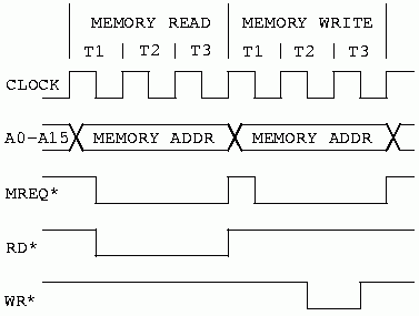
Figure 22 shows a Z80 data read followed by a write. Note that this bus cycle uses only three clock cycles where the M1 cycle used four. In addition to that the timing is more relaxed. This is because we get two and a half clock cycles for the memory access instead of one and a half. The difference is that we aren't doing a refresh operation during these cycles.
For memory access on the Z80 we will control DRAM timing with a combination of MREQ* and either RD* or WR*. We will design the system with a single 30 pin SIMM module. It will be able to support up to a 4MB SIMM. These SIMMs use bi-directional data pins, so we will have to use EARLY-WRITE on the SIMM. We will use a delay line to generate the DRAM timing as we don't have a high speed clock to use with a shift register. We will use CAS before RAS refresh to refresh the SIMM as the Z80 only outputs 7 address lines for refresh. We will be able to use the Z80 to trigger the refresh operation by using the combination of MREQ* and RFSH* to generate our timing. We will also design the memory system to require no wait states from the Z80. With the speed of memories available today, this should be no problem.
Let us examine the Z80 M1 timing, combined with our proposed DRAM timing added in, to see if it looks like everything will fit, and start to get an idea of what speed SIMMs we will need to use. The following diagram will not attempt to be precise, but to put everything in proportion.
For the sake of discussion, we will assume the Z80 to be running at 4 MHz.
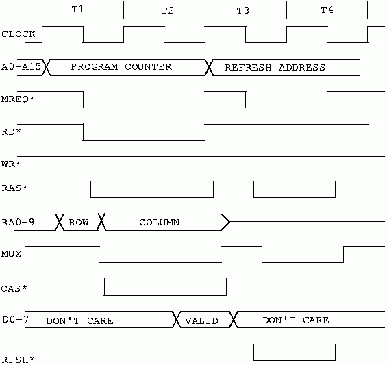
As we can see in figure 23, the available time for memory access during an M1 cycle is one and a half clock cycles. The instruction read is controlled by MREQ*. It begins with the falling edge of the CPU clock in T1 and extends to the rising edge of the clock at the beginning of T3. This sets the worse case access time for the Z80 since, we discovered earlier, a data store/read has two and a half clock cycles. We will design for the M1 cycle, and ignore the data cycle. If our memory system is fast enough for the M1 cycle, it will surely be fast enough for the data cycle.
At 4 MHz the Z80's clock period, or time from rising edge to rising edge, is 250ns. Our MREQ* pulse width at 4 MHz will then be 375ns. With today's memories this is a long time. We don't actually have the full 375ns. The Z80 samples the data on its' data bus on the rising edge of the clock. Data must be stable at the pins of the Z80 CPU chip some time before the rising edge of the clock to ensure that the Z80 reads correct data. In the case of the 4 MHz Z80 this time is 35ns. Also, the Z80 may not make MREQ* active right on the falling clock edge. In the case of the 4 MHz Z80, it could be as long as 85ns after the clock. Since we have to design for the worst case we must subtract 120ns (35+85) from our 375 ns. This still leaves us 255ns to access memory during the M1 cycle. We should be able to easily use 150ns DRAM parts with no wait states with this design.
Notice also from figure 23 that the Z80 always follows the M1 memory fetch with a memory refresh cycle. This refresh cycle is technically part of the M1 cycle, using states T3 and T4. If the Z80 didn't perform a refresh during this time the external bus would simply be idle. In doing the refresh this way, Zilog gave us a no-penalty refresh. That is, refreshing the dram memory uses no memory bandwidth that could have been used for something else. This a gift. You won't see it again. Modern processors utilize the full bandwidth for memory, and refresh must be forcibly inserted into the stream of accesses, thus taking some of the memory bandwidth for refresh.
With the older memories, refresh would be implemented using RAS only refresh. All drams up to the 256K by 1 parts needed this, and some of the 256K parts did as well. If you're working with older parts, I.E. - 4K, 16K, 64K, you MUST implement RAS only refresh. If you are using 256K parts, check the data sheet for the parts you intend to use before you begin. If they will support CAS before RAS refresh, then by all means that is the best way to do it. You will eliminate a lot of parts from the DRAM controller circuit, and a lot of the complexity in the control logic for it.