SX28AC EMI Evaluation: EMI Results and PCB Design Considerations
![]()
Application Note 3
Abdul Aleaf
November 2000
1.0 INTRODUCTION
This report provides a summary of the EMI results for the SX28AC. An independent EMI lab that specializes in EMI testing has taken all the measurements. Based on the results obtained, an analysis of the data is provided and overall PCB design guidelines are given so that the designer can minimize EMI before it becomes a problem.
1.1 Test Types
1.2 Package Types
The footprints for both packages were laid out on the same PCB to get an accurate comparison of the EMI data between the two packages.
1.3 Device Operating Frequency
Measurements were taken using 4 MHz, 12 MHz, and 50 MHz resonators.
2.0 RADIATED EMISSION RESULTS
The SAE J1752 Integrated Circuit Radiated Emissions Measurement Procedure was used to obtain the SX emissions results. This procedure tailors the measurements for an IC (specifically a microcontroller). This SAE Recommended Practice defines a method for measuring the electromagnetic radiation from an integrated circuit. The method uses a standardized IC test board containing the IC being evaluated mounted to a mating port cut in the top or bottom of a 1 GHz TEM cell. One of the TEM cell feeds is terminated with a 50-ohm load and the other one is connected to the input of a spectrum analyzer, which measures the RF emissions over the frequency range of 150 KHz to 1000 MHz.
2.1 Standardized IC Test Board
This special square PCB includes a ground plane, which serves as a shield; the periphery of this shield is tinned to facilitate contact to the edge of the mating hole cut in the top or bottom of the TEM cell. The top side of this board that is inside the test cell is fully shielded except for the IC being evaluated and a narrow strip of vias around the IC. Other required components (such as a resonator) are
located on the other (bottom) side of this board. All SX I/O pins are terminated with 10 K resistors to Vdd and 50 pF capacitors to Vss. The board is laid out to accommodate 28-pin SOIC and 28-pin SDIP packages as well as different oscillator types.
2.2 EMI Test Code
The test routine implements a counter function using a single 8- bit port. Every 100 us, the port output is incremented. After 10 count cycles (256 ms) an LED output is toggled. For consistency, equivalent loop times are maintained (used in European IC Emission Testing).Figure 1 shows the test code flowchart.
2.3 Test Equipment and Conditions
Table 1 shows the completed SAE J1752/3 datasheet.
2.4 Emission Levels
Figures 3 - 6 shows the emission levels for different frequencies and package types.
© 2000 Ubicom, Inc. All rights reserved.
- 1 -
www.ubicom.com
SX28AC EMI Evaluation: EMI Results and PCB Design Considerations
AN-3
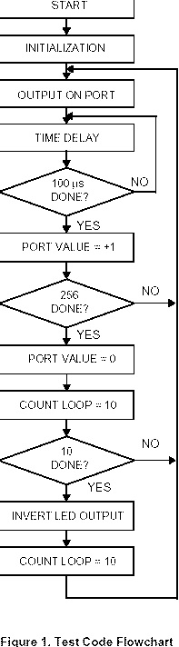
Table 1. Integrated Circuit Radiated Emissions Measurement Procedure (SAE J1752/3 Issued MAR95) 150 kHz to 1 GHz, TEM CELL
SAE J1752/3 DATA SHEET
| TEM cell used: | CE Asst 3274 |
|
|
|
| VSWR OK to 1 GHz: | OK |
|
|
|
| Spectrum analyzer used: | CE Asst# 3053 |
|
|
|
| Cal. OK to 1 GHz: | OK |
|
|
|
| Resolution Bandwidth (RBW): | See setup printout |
|
|
|
| Video Bandwidth (VBW): | See setup printout |
|
|
|
| Pre-amp model: | HP 8447D Ass# 3031 |
|
|
|
| Gain: Cal. OK to 1 GHz: | OK |
|
|
|
| coax cable type and | 15’ Cal to 1GHz |
| approx. length: | |
|
|
|
| 50 ohm termination for TEM | OK |
| cell verified to 1 GHz: | |
|
|
|
| System gain check | OK |
| (without the TEM cell) | |
|
|
|
| Ambient noise floor level: | -10 dBuV |
|
|
|
| Ambient temperature: | See Data |
|
|
|
| IC supply voltage: | 5V |
|
|
|
| Power supply or battery | Power Supply |
|
|
|
| Type of software used to | Per SAE J1752/3 test |
| exercise the IC: | code |
|
|
|
© 2000 Ubicom Semiconductor, Inc. All rights reserved.
- 2 -
www.ubicom.com
AN-3
SX28AC EMI Evaluation: EMI Results and PCB Design Considerations
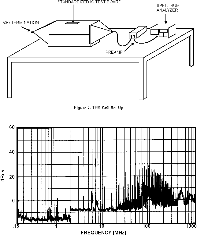
Figure 3. Emission Levels at Device Operating Frequency of 4 MHz - 28 SOIC
© 2000 Ubicom Semiconductor, Inc. All rights reserved.
- 3 -
www.ubicom.com
SX28AC EMI Evaluation: EMI Results and PCB Design Considerations
AN-3
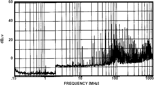
Figure 4. Emission Levels at Device Operating Frequency of 12 MHz - 28 SOIC
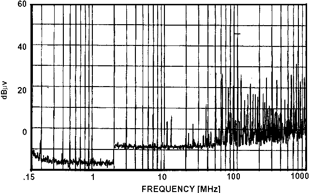
Figure 5. Emission Levels at Device Operating Frequency of 50 MHz - 28 SDIP
© 2000 Ubicom Semiconductor, Inc. All rights reserved.
- 4 -
www.ubicom.com
AN-3
SX28AC EMI Evaluation: EMI Results and PCB Design Considerations
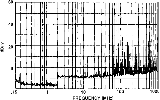
Figure 6. Emission Levels at Device Operating Frequency of 50 MHz - 28 SOIC
© 2000 Ubicom Semiconductor, Inc. All rights reserved.
- 5 -
www.ubicom.com
SX28AC EMI Evaluation: EMI Results and PCB Design Considerations
AN-3
3.0 RADIATED SUSCEPTIBILITY
The SX device was evaluated for susceptibility based on IEC 1000-4-3 (European version EN61000-4-3) specification. The frequency range was 27 MHz to 1000 MHz.
The device did not show any susceptibility. Test setup, test equipment, and test results are attached to this report.
AREA OF UNIFORM FIELD
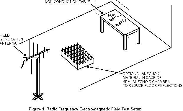
Table 1. Radio Frequency Electromagnetic Field Test Parameters
| COMPANY | SCENIX | DATE |
|
|
||
| EUT | SX28AC COOMUNICATIONS CON- | ENGINEER |
| TROLLER | ||
|
|
||
| DEVICES | SX28AC - SDIP/SOIC | AIR TEMPERATURE |
|
|
||
| SPEC | IEC 1000-4-3 | BAROMETRIC |
| PRESSURE | ||
|
|
||
| LEVEL | 3 V/m, | RELATIVE |
| 1 kHz AM SINE WAVE AT 80% | HUMIDITY | |
|
|
||
| PERFORMANCE | A | |
| CRITERIA | ||
|
|
||
11-24-98 R. O. RAMIREZ
At Compatible Electronics 20 C
104.0 kPa
44%
© 2000 Ubicom Semiconductor, Inc. All rights reserved.
- 6 -
www.ubicom.com
| AN-3 | SX28AC EMI Evaluation: EMI Results and PCB Design Considerations | |||
|
|
||||
| TEST EQUIPMENT | CAL. DATE | CAL. CYCLE | ||
|
|
||||
| ANTENNA: Com Power Biconical, AB-900 | N.C.R. | N/A | ||
|
|
||||
| ANTENNA: Com Power Log Periodic, AL-100 | N.C.R. | N/A | ||
|
|
||||
| AMPLIFIER: Amplifier Research: 75A220 | N.C.R. | N/A | ||
|
|
||||
| AMPLIFIER: Amplifier Research: 100W1000M1 | N.C.R. | N/A | ||
|
|
||||
| SIGNAL GEN.: Giga-Tronics: 6062A | 3/10/98 | N/A | ||
|
|
||||
| TEMPERATURE/HUMIDITY METER: Abbeon HTAB169B | N.C.R. | N/A | ||
|
|
||||
| OTHER: Amplifier Research Field Monitor System, FM2000 | N.C.R. | N/A | ||
|
|
||||
| OTHER: Amplifier Research Field Probe System, FP2000 | 8/12/98 | 1 Year | ||
|
|
||||
| Note: N.C.R. means No Calibration Required. | ||||
|
|
||||
| FREQ. RANGE (MHz) POLARIZATION | RESULT | THRESHOLD (V/m) | COMMENTS | |
|
|
||||
| 27 - 1000 Vertical | PASS | >3 | No susceptibility observed | |
|
|
||||
| 27 - 1000 Horizontal | PASS | >3 | No susceptibility observed | |
|
|
||||
| and lead frame in the package). | ||||
4.0 ANALYSIS OF THE RESULTS
| 1. |
The SX device passes
susceptibility tests per IEC 801-3 specification despite the fact that schmitt
trigger function was disabled on all I/O ports during the measurement. The
schmitt trigger function, if enabled, should help reduce susceptibility further.
It seems the SX I/O pins have a reasonable amount of input capacitance that
allows the device to achieve high EMC tolerance. |
| 2. |
Near field probing indicates
that modulation of the power supply lines by high frequency switching in
the SX device is reduced due to placement of Vdd and Vss pins close to each
other and on one side of the package. This leads to a small trace length
to the decoupling capacitor and also the smallest radiating area. The SO
package is particularly advantageous in this case. |
| 3. |
The rise and fall times of
the port drivers seem to be low enough to keep the radiated interference
at reduced level due to port switching. Measurements were taken with the
device being held in RESET and the results were compared with emission levels
obtained during output switching. No significant difference was observed.
Typically CMOS output stages may cause “shoot through” current
to be drawn when switching, if the high-side and low-side drivers are both
on at the same time. The SX I/O ports have slew rate control (gradual turn
on) circuitry that helps control the “shoot through”
effect. |
| 4. |
The maximum emission levels
are observed at the harmonics of the operating frequency. For example, for
an operating frequency of 12 MHz, the peak emission level is at 48 MHz. For
50 MHz operation, the peak level is at the 100 MHz band. |
| 5. |
The SDIP package seems to
be noisier than the SOIC at certain frequency bands. The SOIC package provides
shorter connection from the chip die to the PCB and reduces the antenna effect
(short bonding wires |
5.0 GENERAL GUIDELINES FOR PCB LAYOUT AND CONSTRUCTION
5.1 Suppression of Interference on the Supply Line
| 1. |
Current and voltage peaks
are the most common causes of EMI. Use of proper decoupling capacitors between
Power and Ground at the power source to the board as well as on the SX Vdd
and Vss pins may help. It is also important to evaluate the proper capacitor
type, frequency response, placement, output load effect, and size. |
| 2. |
The decoupling capacitor
by itself may not be able to significantly reduce the radiated interference.
Because the inductance causing the interference has already been formed,
to a large extent by the packages of the ICs and the connection to the capacitor,
significant improvement cannot be achieved by simply connecting in parallel
several capacitors of different values. Of greater concern is preventing
the current causing the disturbance from reaching the other parts of the
circuit. This can be achieved by introducing an inductor behind the decoupling
capacitor, which represents a sufficiently high resistance at high frequencies.
The impedance of the inductor could be limited at high frequencies by a resistor
of 50 Ohm connected in parallel to the inductor. A more cost effective approach
is to run a small trace from Vdd to a capacitor, and a larger trace from
the capacitor to the SX device. |
© 2000 Ubicom Semiconductor, Inc. All rights reserved.
- 7 -
www.ubicom.com
SX28AC EMI Evaluation: EMI Results and PCB Design Considerations
AN-3
5.2 Reducing the Power and Ground Loop Area
The long supply lines with the relatively large areas that these lines surround may form an effective antenna. At the frequencies present, an unacceptable level of interference may be radiated. A grounded area under the SX device must be connected to the Vss pin. In addition, the ground area should be tied to the ground plain with multiple vias. This ground area ensures that the major part of the field lines emanating from the SX are concentrated between the SX and the ground level.
5.3 Oscillator Considerations
| 1. |
The oscillator circuit needs
to be analyzed with respect to the flow of significant current to determine
where the interference suppression is necessary. |
| 2. |
Since the SX power and ground
pins are on the opposite side of the package from the one for the oscillator
pins, one needs to evaluate the effect of the larger loop created as a result
of connecting the oscillator capacitors to the ground. This large loop will
result in larger amount of current flow in the oscillator resonant circuit.
The creation of a ground plane underneath the chip (mentioned above to reduce
the power line loop) will help shorten the loop effect. In addition, it will
be useful to run the capacitor ground connection close and in parallel to
the clock input and output signals. If ground area underneath the chip is
not available, the capacitor should be directly connected to the SX ground
pin through a short and independent trace. Figure shows the recommended
oscillator circuit layout. |
| 3. |
The shape of the oscillator
signal should be observed with a low capacitance FET probe to identify any
ringing. The oscillator signal should look smooth. Impedance matching techniques
can be employed to smoothen the oscillator signal. |
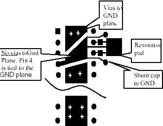
Figure 1. Oscillator Circuit Layout
5.4 Handling High Speed I/O Signals
| 1. |
High speed signals should
be close to the ground plane or ground signals. High speed signal wires and
their returns should be as short as possible and put in the smallest possible
area. As mentioned in Section 4.0, the SX output drivers have slew rate control
(gradual turn on), it may still be beneficial to slow I/O pin transition
further by adding 10 pF capacitors on the I/O pins. This is useful in
applications that involve large amount of data transfer into/out of the SX
device. |
| 2. |
High speed signals should
be shielded and kept away from other signals, in order to avoid crosstalk,
particularly on high resistance and level sensitive tracks. The tracks should
be routed sufficiently far apart or run parallel to a track connected to
the system reference voltage, usually ground, to provide
shielding. |
5.5 General Considerations
| 1. |
If the PCB contains both
analog and digital circuits, there should be separate analog and digital
power supplies and grounds. |
| 2. |
Single point connection of
tracks for analog ground and power supply. In order to avoid different potentials
a galvanic connection at only one point is desirable. Track loops should
be avoided (also less susceptible to interference). |
| 3. |
Large ground plane. If the
size of the ground plane is increased, the radiating area due to current
loops will be reduced. Additionally, the capacitance to ground of the digital
lines is increased which could lead to an increase in the interference caused
by switching currents. |
| 4. |
Low inductance connections.
The use of short connecting wires results in a reduction of any inductive
voltage spikes as Vi = L.di/dt at constant di/dt when switching. |
| 5. |
If the board physical layout
permits, it is beneficial to keep the power connector (power source to the
board) and other connectors (such RS-232) on the same side of the
board. |
| 6. |
On a two-sided board, if
the back side is copper poured, try to keep this side free of components,
traces, and “cuts” as much as possible to leave more ground metal
area. |
| 7. |
Using a multi-layer board
can lead to reduction in emitted interference. The improvement is due to
the reduction in track length and the reduction of Vdd to ground impedance,
for example if Vdd/ground grid is used. |
© 2000 Ubicom Semiconductor, Inc. All rights reserved.
- 8 -
www.ubicom.com
SX28AC EMI Evaluation: EMI Results and PCB Design Considerations
AN3
Lit.#: AN03-03
Sales and Tech Support Contact Information
For the latest contact and support information on SX devices, please visit the Ubicom website at www.ubicom.com. The site contains technical literature, local sales contacts, tech support and many other features.

1330 Charleston Road, Mountain View, CA 94043
Contact: Sales@ubicom.com http://www.ubicom.com Tel.: (650) 210-1500 Fax: (650) 210-8715
© 2000 Ubicom, Inc. All rights reserved.
- 9 -
www.ubicom.com
| file: /Techref/SCENIX/sxemi.htm, 36KB, , updated: 2005/8/17 13:52, local time: 2024/8/31 17:08,
18.119.166.31:LOG IN
|
| ©2024 These pages are served without commercial sponsorship. (No popup ads, etc...).Bandwidth abuse increases hosting cost forcing sponsorship or shutdown. This server aggressively defends against automated copying for any reason including offline viewing, duplication, etc... Please respect this requirement and DO NOT RIP THIS SITE. Questions? <A HREF="http://www.sxlist.com/TECHREF/SCENIX/sxemi.htm"> sxemi</A> |
| Did you find what you needed? |
Welcome to sxlist.com!sales, advertizing, & kind contributors just like you! Please don't rip/copy (here's why Copies of the site on CD are available at minimal cost. |
Welcome to www.sxlist.com! |
.